
Deep|TSEM: SiPho Capacity Inflection Drives Multi-Fold Growth Cycle

Industry Context: The Optical Interconnect Revolution
AI data center compute clusters are currently scaling from thousands of GPUs to tens or even hundreds of thousands of nodes. At this magnitude, traditional copper interconnects are reaching severe physical limits; once transmission rates hit 800G and above, transmission reach shortens dramatically while power consumption escalates exponentially. To bypass these constraints, Silicon Photonics (SiPho) is becoming the essential backbone for AI Networking.
As of 4Q25, Tower Semiconductor’s Silicon Photonics business has emerged as the company’s primary growth engine. Revenue doubled from $106mn in 2024 to $228mn in 2025, achieving an annualized revenue run rate exceeding $360mn by the end of 2025. As the industry transitions from 400G/800G toward 1.6T, Tower has positioned itself as the lead supplier of 1.6T Silicon Photonics wafers. We believe Tower is currently the premier SiPho PIC (Photonic Integrated Circuit) foundry with a distinct competitive lead. Among major competitors, Malaysia’s Silterra lacks significant expansion capacity, while SiPho offerings from UMC, GlobalFoundries (via the AMF acquisition), and STM still trail Tower by a wide margin.
The following table compares interconnect technology parameters:

The TDP (Thermal Design Power) of AI server racks, such as the Nvidia GB200 series, has jumped from 700W in the Hopper generation to over 1,200W, necessitating the adoption of liquid cooling and more efficient optical interconnects. Within these environments, SiPho facilitates higher speeds while maintaining system scalability under strict thermodynamic limits.
On February 5, NVIDIA and Tower Semiconductor established a strategic partnership focused on high-speed optical interconnects for AI data centers. Tower will leverage its SiPho process platform to manufacture 1.6T-class SiPho optical engines and modules for NVIDIA’s next-generation networking architecture, optimized for NVIDIA’s specific protocols. This collaboration aims to resolve bandwidth and energy efficiency bottlenecks during the Scale-out phase of massive GPU clusters.
Separately, we have highlighted the rapid progression of Optical Scale-Up, with volume production expected to commence in 2027. Delivering over 10x the optical bandwidth of traditional Scale-Out, Optical Scale-Up—whether implemented via pluggable modules, NPO, or CPO—will significantly drive demand for SiPho PICs.
Alibaba’s UPN512 (a 512-xPU optical scale-up super-node) validates the migration of optics from scale-out networking into the scale-up core domain, as LPO/NPO and other near-packaged solutions achieve system-level economics. Consequently, optics is evolving from a mere bandwidth expansion tool into a foundational infrastructure component for scale-up architectures.
For SiPho, this shift directly expands the long-term TAM. Scale-up environments demand higher port densities, extreme bandwidth, and stricter power budgets—requirements natively addressed by high-integration SiPho PICs and linear drive solutions. SiPho’s penetration is moving beyond “incremental replacement” to potentially becoming the default interconnect standard for next-generation AI super-nodes.
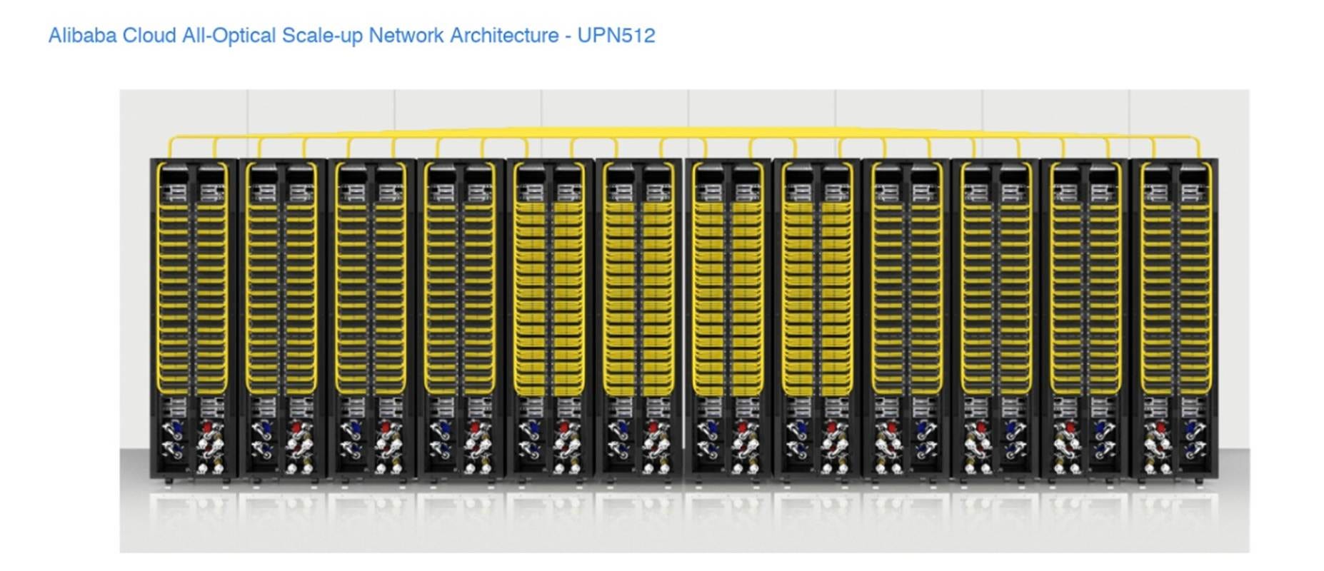
SiPho based 3.2T NPO module by Alibaba
Technology Deep Dive
Tower’s PH18 platform is the industry’s most mature 200mm Silicon Photonics foundry process, primarily centered at its Newport Beach, California fab. Through partnerships with EDA vendors like Cadence, Synopsys, and Luceda, Tower provides full PDK support to ensure first-pass success for customer designs. The platform also offers Multi-Project Wafer (MPW) services, which significantly lowers the barrier to entry for Silicon Photonics startups.
In late 2024, Tower officially introduced 300mm Silicon Photonics foundry services, optimized for 1.6T applications through several key improvements:
Waveguide Loss Optimization: Employs industry-leading low-loss silicon and silicon nitride processes essential for long-distance and multi-stage optical paths.
OSAT Compatibility: 300mm wafers are designed for automated routing with global OSAT platforms, which is critical for reducing costs in 1.6T modules involving wafer-level packaging and micro-bump connections.
Economies of Scale: A 300mm wafer provides over 2.25x the usable area of a 200mm wafer, offering necessary cost reduction as the transceiver market faces ASP pressure despite high demand.
A key technical differentiator for Tower is its 3D-IC heterogeneous integration technology derived from its BSI image sensor expertise. In CPO architectures, Electronic ICs (EIC) and Photonic ICs (PIC) must be tightly stacked. Using 300mm wafer bonding, Tower can stack different process nodes, such as high-frequency SiGe BiCMOS and SiPho, to minimize electrical paths and parasitic resistance, which is vital for maintaining 1.6T signal integrity.
