Deep|Heterogeneous Integration and Chiplets: The Defining Trends from ISSCC 2026

This article is reproduced with permission from Silicon Talks. This report was written by a friend of ours, and it’s very closely aligned with our line of research. We’ll be releasing a few more deep dives on optics names soon.
New integration technologies are reshaping the compute landscape in real time. As recently as ISSCC 2020, chiplet-related papers appeared only sporadically. Fast-forward to today, and chiplet architectures have penetrated virtually every ISSCC technical track: digital, compute, memory, sensing, display, with heterogeneous integration also making inroads into Power, Bio, and RF. This year, papers on heterogeneous integration and chiplets surged in volume.
This article provides a systematic review of how chiplet and heterogeneous integration technologies evolved at ISSCC 2026, and examines where the field is headed.
Compute Carriers: From 2.5D to 3.5D Integration
Large-die manufacturing runs up against a hard physical ceiling, the reticle size of the lithography tool, which caps the maximum area of any single chip. Meanwhile, demand for compute is scaling relentlessly. Heterogeneous integration design tackles this by projecting power the way a carrier strike group does: by assembling multiple chiplets through advanced packaging and vertical interconnects, breaking through the area bottleneck of a monolithic die.
The opening paper at this year’s ISSCC, AMD’s MI350 series, delivered a textbook demonstration. This carrier-class compute chip showcased the potential of a 3.5D architecture: using a silicon interposer and hybrid bonding to stack compute units, memory, and interconnect fabric in separate layers, integrating tens of billions of transistors within a constrained package footprint. This is not simply about going bigger; it is a fundamental rearchitecting of how compute silicon is assembled, setting a new paradigm for AI accelerators.
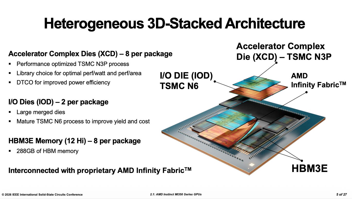
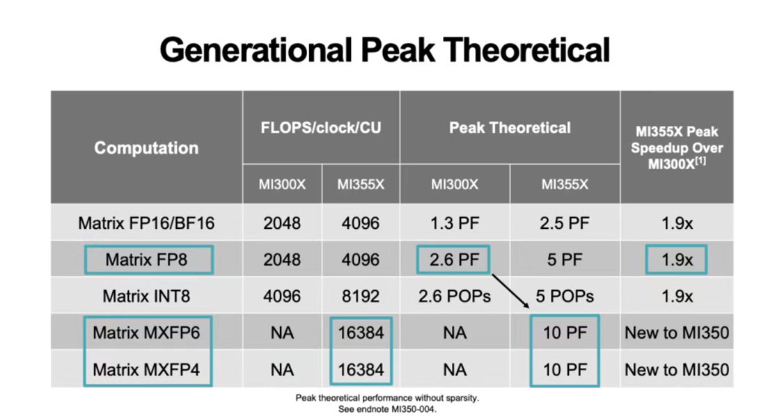
Compared with the MI300, the MI350 takes a markedly more aggressive integration approach. The four 200 mm² active-interposer segments of the MI300 have been consolidated into two, substantially simplifying inter-segment routing and eliminating much of the complex crossing logic. Vertical interconnect bandwidth is up 2.2×, and on-die SRAM capacity has grown 2.5×, allowing more of the parallel-compute latency to be hidden inside data-buffering pipelines, a throughput-first design philosophy in the truest sense. The MI350 no longer measures its performance in teraFLOPS; it leaps straight to the 10-petaFLOPS class. That kind of density and energy efficiency redefines the ceiling for what a single compute package can deliver.
Next, Korean startup Rebellions unveiled the R100, combining four NPU dies, four HBM3E stacks, and four power-integrity decoupling-capacitor chiplets, delivering 2 petaFLOPS of aggregate compute.
The key innovation lies in a distributed mesh communication fabric optimized for multi-die, multi-core topologies, providing a complete interconnect solution tailored to large-model workloads. Relative to conventional mesh links, the R100 introduces several structural refinements and offers a forward-looking vision for rack-scale I/O die design. This architecture underscores an important trend in the chiplet era: achieving a new equilibrium between compute scaling and energy efficiency through hierarchical separation and co-optimization of intra-chiplet, inter-chiplet, intra-package, and inter-package interconnects.
Microsoft followed with MAIA 200, its custom inference chip, demonstrating the kind of silicon muscle that hyperscalers can now bring to the table.
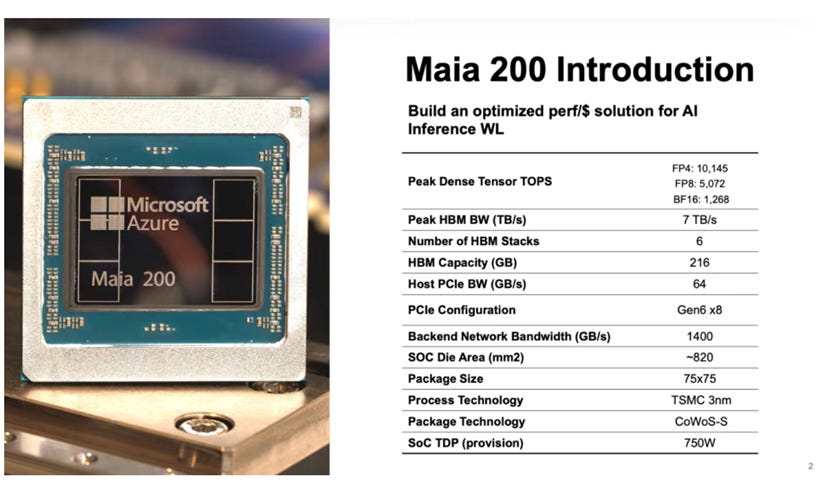
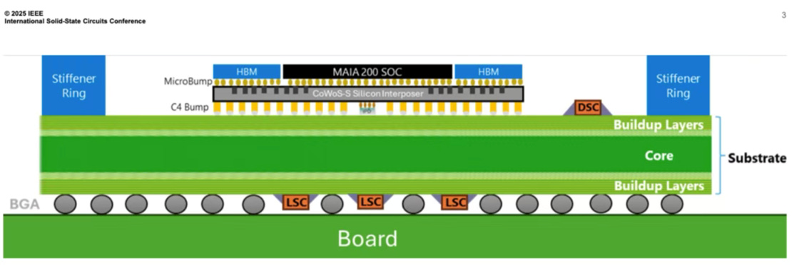
Built on a 3 nm process node, MAIA 200 delivers 10-petaFLOPS-class throughput at a power envelope of 750 W, which, predictably, makes thermal dissipation and power integrity far more challenging. To address this, the package incorporates a multi-layer capacitor strategy: deep-trench capacitors (DTC) integrated on the interposer, integrated passive devices (IPD) on the interposer backside, and land-side decoupling capacitors on the substrate backside. This layered approach reflects differentiated management across distinct thermal and power domains. It highlights a critical trend in heterogeneous integration architecture. Once power dissipation pushes past the several-hundred-watt mark, power integrity and thermal management can no longer be treated as afterthoughts. They must be co-designed and holistically optimized across the chip, package, and system levels.
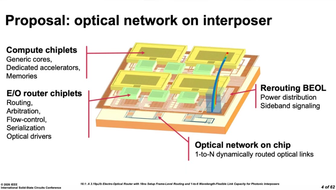
Optical and Terahertz: New Frontiers for 3D Integration
Conventional package-level interconnects rely on wireline electrical signaling, using standards such as UCIe to shuttle data between chiplets. This year’s Wireline and Memory Interface sessions featured several impressive UCIe/chiplet interconnect designs. But as package footprints expand by orders of magnitude beyond tens of square millimeters, the limitations of electrical signaling become hard to ignore: attenuation, crosstalk, and power consumption all scale unfavorably. Technologies once reserved for data-center-scale optical interconnects and terahertz communications are now migrating down to the 3D-package level. This is not merely a technology transfer. It marks a paradigm shift in how chiplets communicate.
Let us start with NVIDIA’s co-packaged optics (CPO)
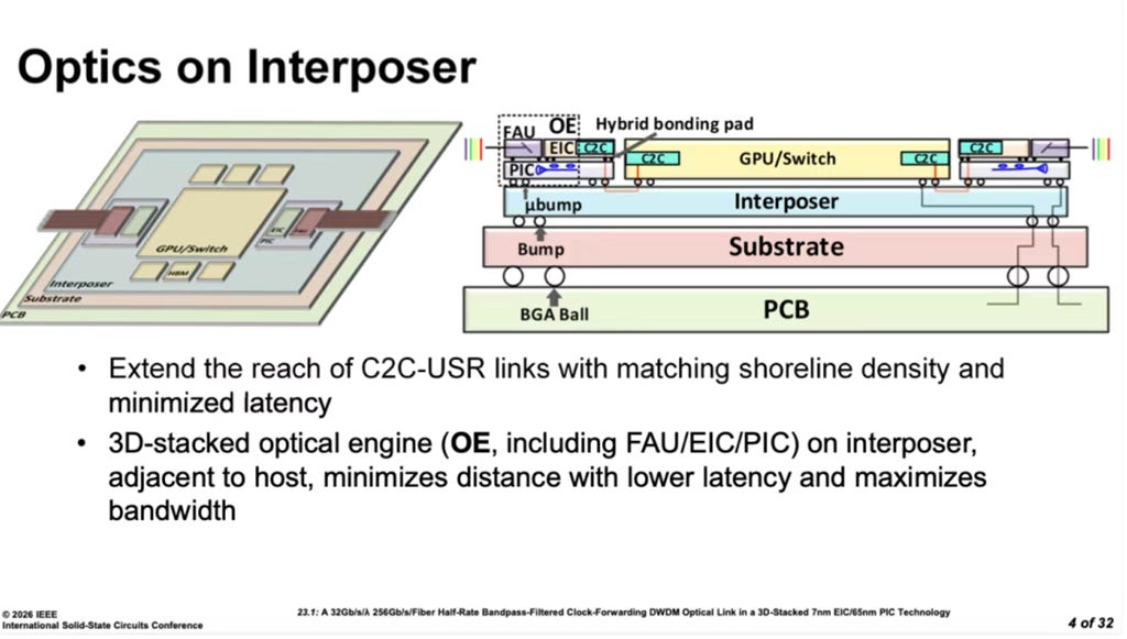
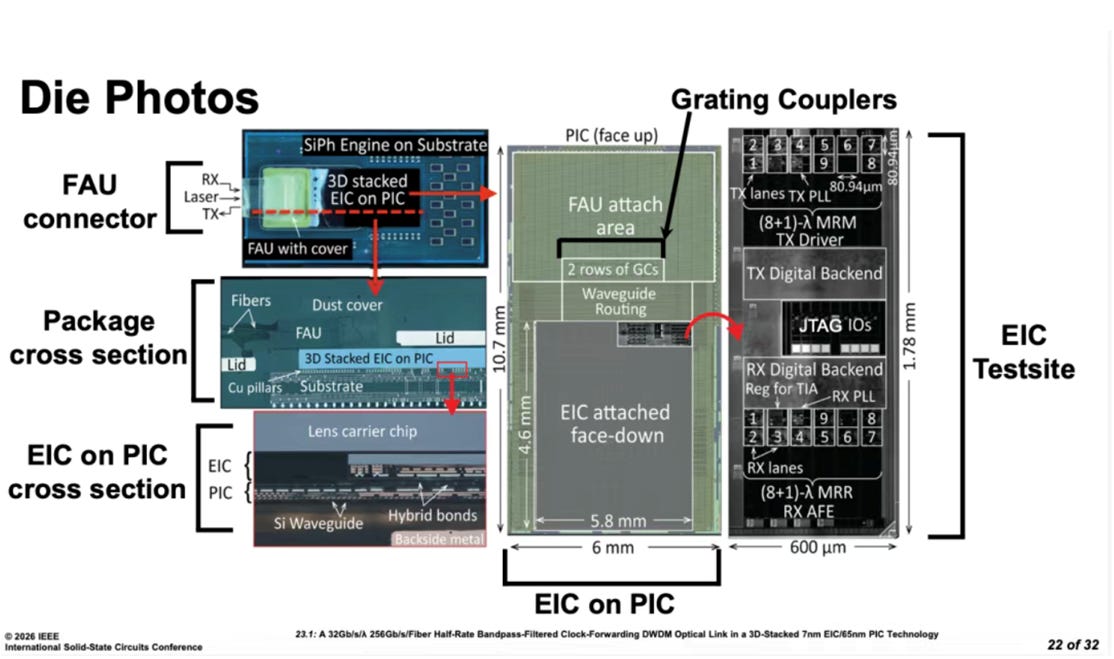
NVIDIA’s heterogeneous opto-electronic integration stacks a 3 nm electrical-interconnect die on top of a 65 nm optical-interconnect die through 3D bonding, forming a complete co-packaged optics (CPO) interface. This combination enables high-speed, medium- to long-distance interconnects for GPUs or switch chips. The breakthrough: rather than forcing heterogeneous process nodes into a single die, NVIDIA lets each node play to its strengths: 3 nm handles high-speed digital logic. In comparison, 65 nm handles photonic conversion and analog circuits. This “right tool for the right job” architecture provides a more efficient pathway for optical interconnects over moderate distances and opens new possibilities for intra-data-center high-bandwidth links.
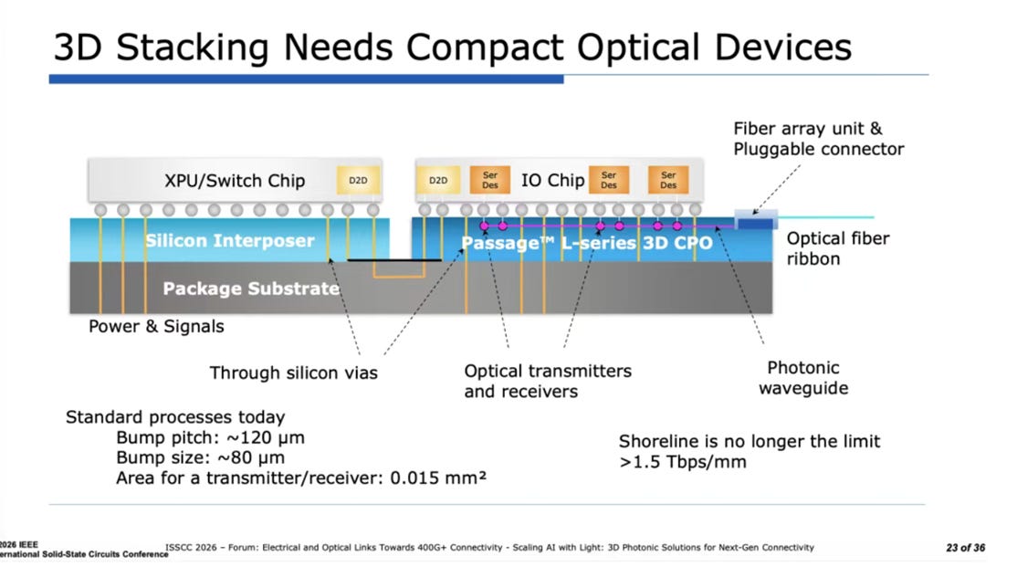
Lightmatter presented a similar concept at this year’s Forum session, along with its Passage product line.